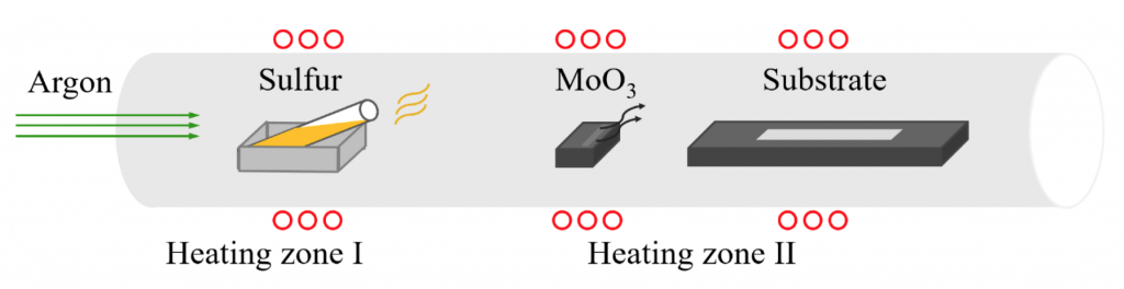
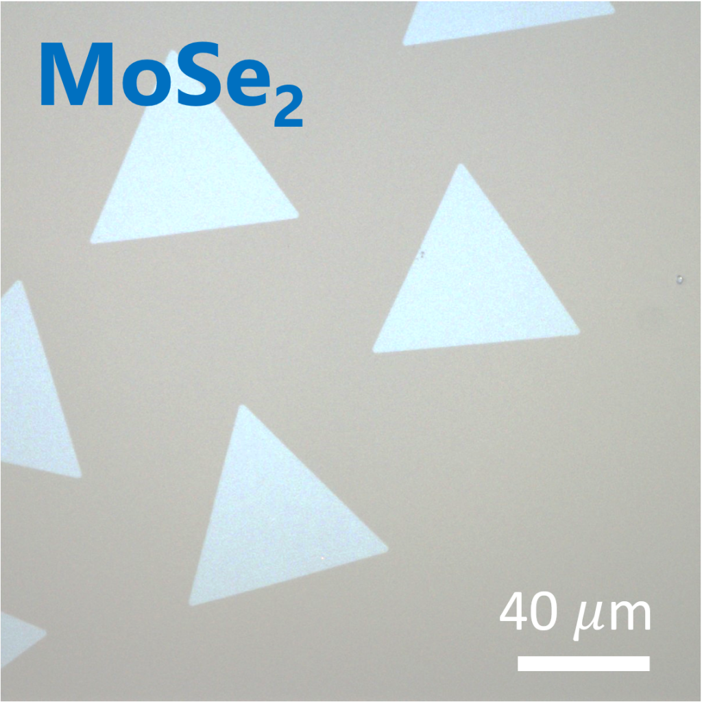
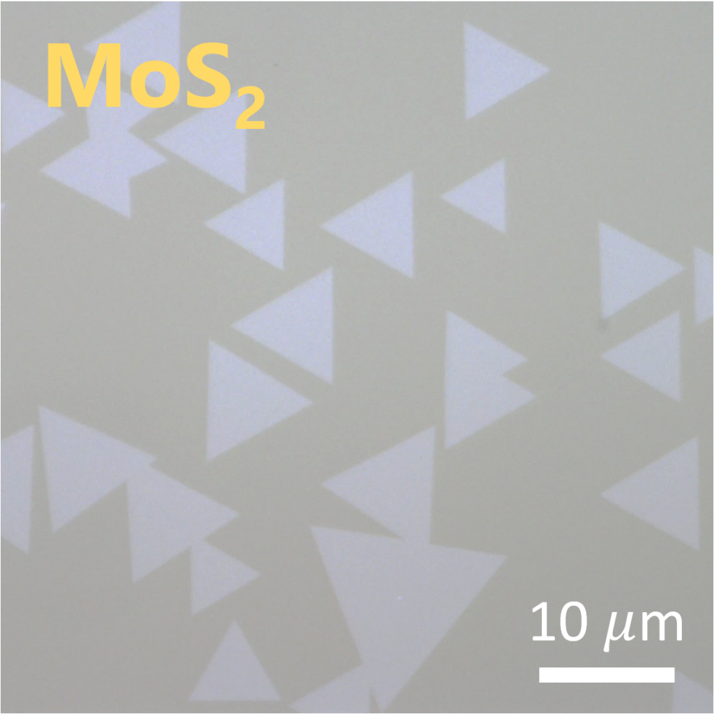
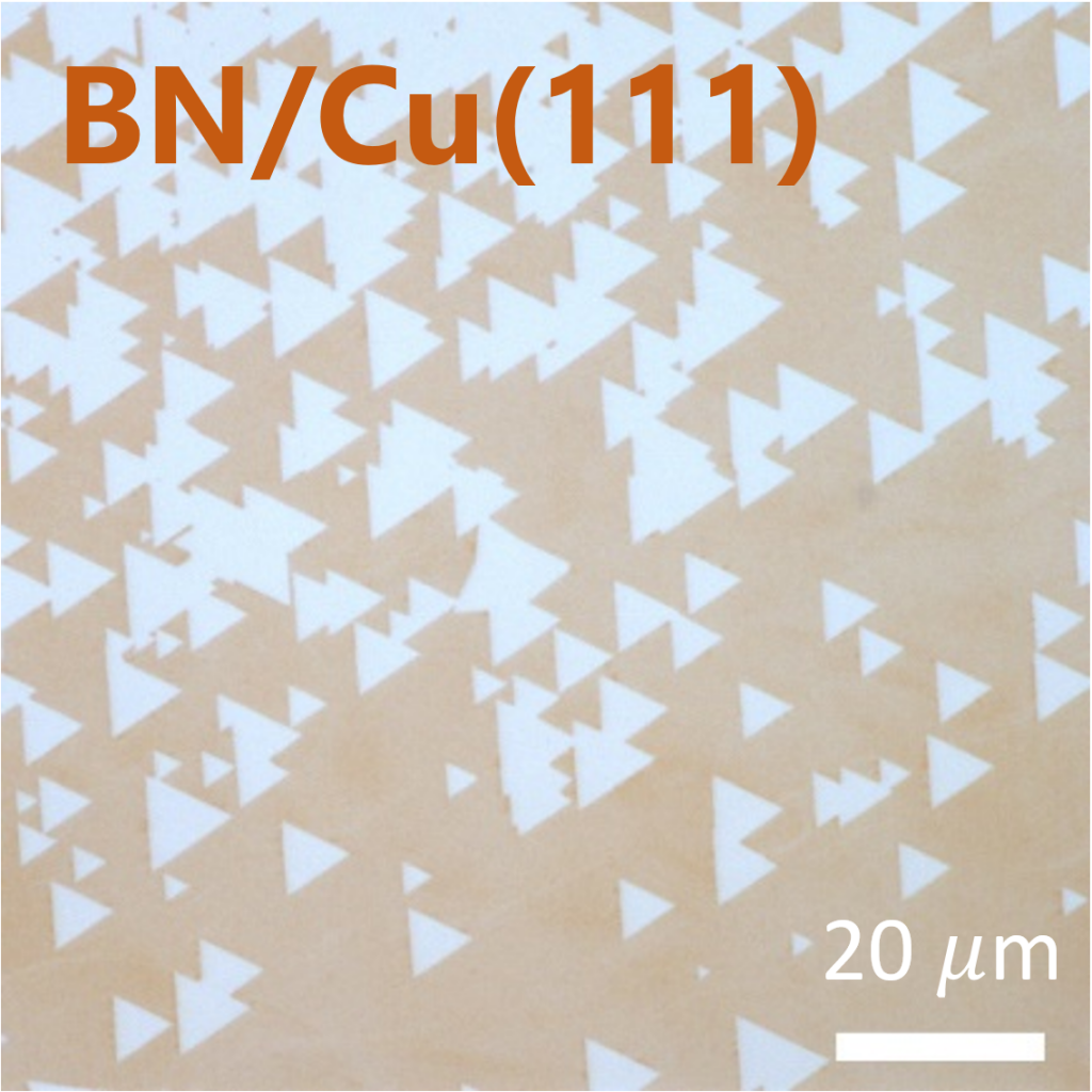
The emerging of two-dimensional (2D) materials with wide range of electrical and optical properties has attracted tremendous research interest. 2D atomic layer in the form of semiconductors (TMDs), insulators (h-BN) and semi-metals (graphene) thus far have been widely investigated. For the sake of further study in 2D materials, the reliable synthesis is essential. We dedicate to developed controllable, large-area and high quality 2D materials by chemical vapor deposition (CVD) methods. The highly crystalline monolayer TMDs, including MoS2, MoSe2, WS2 and WSe2, with crystal size in the range of 20 μm to 200μm can be obtained on the sapphire substrate. We also develop the cold-wall CVD system for the synthesis of wafer scale and uniform TMDs. Highly oriented monolayer TMDs in two specific orientation aligned with sapphire substrate can be achieved by precisely manipulating the growth conditions. In our latest work, the wafer-scale single crystalline h-BN can be successfully obtained on the processed copper wafer by CVD methods. (see publication for more information.)